SMD refers to Surface Mounted Devices, and SMD LED PCB is increasingly favored by LED manufacturers as surface mount technology (SMT) evolves. PCB is the core part of SMD LED, and having a deeper understanding of SMD LED PCB will help to promote the innovation and development of LED products. Due to small size, design flexibility and high durability, SMD LEDs are extensively used in various electronic products. Therefore, in this post, we elaborate on almost all the aspects of the entire SMD LED PCB, regarding its definition, types, benefits, applications and manufacturing process, to help you make the best of SMT technology. OK, let’s go straight in.
What means SMD LED PCB

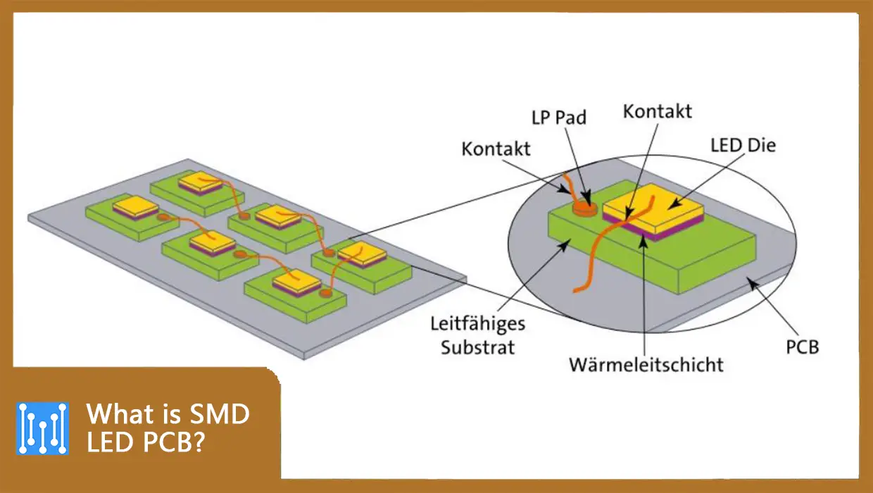
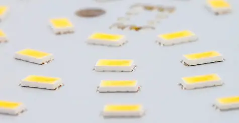
SMD, the abbreviation for Surface Mounted Devices, is a new type of high-power LED light. SMD LEDs are soldered directly to the surface of the PCB board through tiny metallic contacts. They rely on surface mount technology (SMT), no wires, no cutting or drilling into the board. Compared to the previous technologies, SMD LEDs are characterized by compact size, high efficiency, durability and cost-effectiveness, and are therefore the most preferred in the LED market.
Common types of SMD LED PCB
There are a wide variety of SMD LED PCBs available on the market, which are suited to various applications. Among them, the most common types are as follows:
Single-sided SMD LED PCB
It is a special type of PCB because it only contains circuitry on one side and electrical parts on the other side. It consists of a substrate, and in order to protect it, manufacturers often utilize copper as the electrical conductor. Typically, solder masks are applied over the copper layer. Plus, silkscreen coats are used to mark the LED components on the PCB board. Compared to other LED PCB types, single-sided SMD LED PCBs are more cost-effective and easier to manufacture.
Double-sided SMD LED PCB
Both sides of the substrate of double-sided PCBs need to be coated with conductive materials and fused with the electrical components. Additionally, they are preferred over single-sided PCBs due to their greater design flexibility, higher heat dissipation and reliability, and cost-effectiveness. Surface mount technology allows one end of the circuit to be connected directly to the other through holes in the board, saving a lot of space.
Multilayer SMD LED PCB
Compared to double-sided PCB, multilayer SMD LED PCB has more powerful functions. It consists of two or more layers of substrates, each layer of which is separated into single sheets by insulating materials. In terms of space saving, multilayer SMD LED PCBs can save more space than double-sided ones. The number of layers of multilayer SMD LED PCBs can be up to ten or more, which works well for the invention of machinery.
Rigid SMD LED PCB
Several layers of the PCB board are rigid, making it ideal for making fracture-resistant materials. Manufacturers typically use fiberglass as the substrate layer for rigid SMD LED PCBs. FR4 works as the main base material, providing sufficient rigidity and stiffness for the PCB board.
Flex SMD LED PCB
Since the substrate of this PCB is flexible, manufacturers can form it into the desired shape in practical use, providing them with greater design flexibility. However, they are a bit less cost-effective as compared to rigid PCBs.
Rigid-flex SMD LED PCB
This kind of PCB board combines the characteristics of both flexible PCB and rigid PCB. Rigid-flex SMD LED PCBs allow wooden and flexible PCBs to be joined together, which is not possible with other PCBs.
Benefits of using surface mount technology
Most manufacturers today use SMT technology to accommodate automated PCB assembly and mass production. Let’s explore some of the benefits of using this technology:
Small size
SMT technology enables to create smaller sized PCB boards by placing components more closely on the board. This means that SMD designs can be more lightweight and compact.
Design flexibility
For greater functionality, manufacturers can combine through-hole and SMT technologies for PCB building. SMDs can co-exist with through-hole components on the same PCB board, offering greater flexibility in PCB materials and designs.
Component placement autocorrect
When the surface tension of molten solder forces components to align with solder pads, small errors in component placement are automatically corrected.
EMC compatibility
SMT can achieve better Electromagnetic Compatibility (EMC) with lower radiated emissions because it provides a smaller radiation loop area, which is further attributed to its compact package and lower lead inductance.
Cost
Compared to its through-hole counterpart, SMT technology needs less time to set up for production. This is because the assembly process does not require drilling holes on the PCB board, resulting in lower initial costs.
Higher component density
Manufacturers can achieve much higher component density by placing components on both sides of the PCB board. As a result, the number of components per unit area and the number of connections per component increases.
Higher circuit speeds
SMT offers higher circuit speeds since PCB boards made with this method are more compact. It is due to this important reason that most manufacturers tend to adopt this method.
High frequency performance
SMT technology leads to high frequency effects that are better and more predictable than other counterparts. The resistance and inductance at the connection become lower, which mitigates the unwanted consequences of RF signals.
Stability
SMT has better stability and mechanical performance under shake or vibration conditions.
Limitations of using surface mount technology
Its smaller size and lead spaces make component-level repair and manual prototype assembly more difficult.
- SMT technology cannot be used directly to mount components for breadboards.
- Manufacturers can not assure that the solder connections for SMDs are not damaged by potting compounds when going through thermal cycling.
- SMT technology does not work well for high-power or high-voltage parts, such as power circuits.
- SMT technology is not reliable when it comes to use as the sole attachment method for parts that are often subjected to mechanical stress, such as connectors.
Applications of SMD LED PCB
SMD LED PCBs are commonly used in the LED lighting industry and it mainly include:
Automotive industry
You can commonly find SMD LED PCBs in automotive parts such as indicators, brake lights, headlights, digital displays, transmission sensors, power relays, ECU control modules, etc. Thanks to their low manufacturing cost and durability, the service life and value of the vehicle are improved. That is why SMD LED PCBs are particularly favored by the automotive industry.
Telecommunications sector
Owing to their impressive heat dissipation capabilities, manufacturers prefer SMD LED PCBs as indicators and displays for telecommunication equipment. By using this kind of PCB, you don’t need to worry about device failure due to overheating. Thanks to their design flexibility, the versatility of the device can be easily realized.
Medical sector
SMD LED PCBs play an immense role in medical applications. Due to their enhanced efficiency and brightness, they are able to provide great visibility for physicians. SMD LEDs are therefore the lighting tool of choice in surgical and medical examination applications. The longer service life and better heat transfer capabilities of SMD LED PCBs make medical equipment more durable and can be used repeatedly in various medical settings.
Computer technology industry
SMD LED PCBs are extensively used in the computer technology industry, and are commonly found in LED displays and indicators within desktops and laptops. With good thermal conductivity, SMD LED PCBs overcome the thermal sensitivity of computer devices, making them the perfect candidate for LED lighting applications within computers.
Additional use cases
On top of the four applications listed above, some other use cases are given below in number:
- LED grow Light
- LED street light
- LED decorative light
- LED solar lighting
- Traffic and signal light
- Airport runway lighting
- Flashlight
- Lantern
The manufacturing process of SMD LED PCB
Since many manufacturers are inquisitive about the manufacturing process of SMD LED PCBs, the following outline gives the detailed steps involved in this process.
Material preparation and examination
The preliminary stage involves selecting the SMD and designing the PCB. The PCB board typically contains flat pads without holes, known as solder pads, which are commonly made of silver, tin-lead, or gold-plated copper. It is imperative to carefully examine the materials involved in the manufacturing process to make sure there are no flaws.
Stencil preparation
The manufacturer also needs to prepare the stencil, with its role to provide a fixed position for the next solder paste printing process. Besides, the stencil is produced depending on the designed positions of solder pads on the PCB board.
Solder paste printing
At this critical phase, the manufacturer will apply solder paste to the PCB with the stencil using a squeegee at an angle ranging from 45°to 60°. Solder paste, normally a mixture of flux and tin, is used to attach the SMD to the solder pads on the PCB. In SMD LED PCB manufacturing, a reflow oven is a common surface mount equipment used to place the SMD on the PCB.
SMD placement
The process proceeds to load the printed PCB into pick-and-place devices. The SMT placement machine uses a vacuum pipette or gripper nozzle to remove each component from its packaging and place them in the correct position on the board. PCBs are carried on conveyor belts, while electronic components are quickly and accurately placed on them by machines. MOKOLight’s high-precision SMT production machines can assemble up to 10,000 components per hour.
Reflow soldering
After SMDs are placed, it’s time to convey the board into the reflow soldering oven, and proceed them to the following zones for soldering.
Preheat zone: the PCB first enters the preheat zone in the oven. This process gradually heats the board and all the components attached to it.
Soak zone: in this zone, the board will maintain a constant temperature between 140°C and 160°C, lasting for 60 to 90 seconds.
Reflow zone: next, the board will enter a zone where its components are soldered to the pads on the PCB by wire bonding. To melt the tin within the solder paste, the temperature of the board rises at a rate of 1.0°C-2.0°C per second to as high as 210°C-230°C. During this process, the surface tension of the molten solder assists in keeping the components in place.
Cooling zone: to prevent joint defects, the manufacturer needs to pass the board through this final section, where the solder freezes as soon as it exits the heating zone.
If the PCB board is double-sided, you can repeat the printing, placement and reflow process with solder paste or glue to hold the SMDs in place.
Clean and inspection
After soldering the boards, you need to clean and examine them to make sure they are devoid of any flaws. If you spot a defect, rework or repair it, and then store the product. The equipment used for SMT inspection on the market typically includes magnifying lenses, AOI systems, flying probe testers, X-ray and laser, etc.
SMD LED PCB manufacturing&assembly services from MOKOLight
SMT technology makes LED PCB production much easier and helps save LED manufacturers time and money. MOKOLight offers one-stop LED PCB manufacturing and assembly services for massive applications in a variety of industries. We have extensive experience both in surface mount and through-hole technology. With efficient and automated production processes, we are able to consistently deliver quality LED PCB boards on time that exceed your expectations and fit your budget. You can count on our top-class quality and unparalleled service. If you have needs or questions regarding SMD LED PCBs or other types of PCBs, you can contact us freely.