With the increasing demand for LED lights in commercial and residential sectors, LED light manufacturing industry is booming. As a result, a wide variety of LED lighting products have emerged on the market. And more and more people are exploring or paying attention to the process of LED light manufacturing. This article will take you through a quick look at the differences between LED lights and conventional lights, the material and equipment required for LED light manufacturing, and what the process of LED light manufacturing is like. Let’s dive in right now.
Background: LED Lights VS Conventional Lights

LED or light-emitting diode is a semiconductor device that will emit light even when a small current passes through them. Compared to conventional lighting systems, it is not only different in design, but also different in the way it creates light. Traditional lamps emit light by connecting to a power source with a wire. The heat generated by heating up the wire is converted to light. LED lights, on the other hand, produce light by exciting the movement of electrons rather than by heat.
As opposed to traditional incandescent and fluorescent lamps, LED lights consume less electricity, produce less heat, as well as have a longer operating life and a higher cost of ownership. In addition, LED lights are available in a wide variety of types and colors and can provide better light quality. That’s why LED lights are popular in both domestic and foreign markets and have gradually replaced CFL, incandescent lamps and other traditional light bulbs.
Basic Components of LED Lights

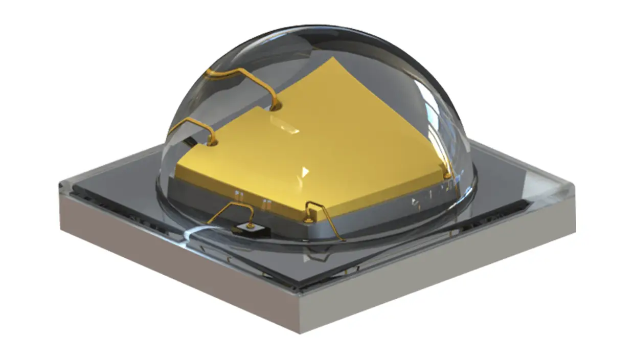
The core component of LED lights is a tiny chip with a layer of semiconductor layer. One or multiple chips are mounted on a heat sink covered by a lens, which results in a device 7 to 9 millimeters thick that has a variety of usages. The LEDs are then mounted on a programmed circuit board that can control the light, including light intensity, light color and light sensing. To control the heat generated by the LEDs, the circuit board is placed on another heat sink. Finally, the system is encapsulated in a lighting fixture or bulb.
Design of LED Lights
More creativity is needed in the design of LED lights. Before LED light manufacturing, there are some optical properties such as the color temperature, brightness and efficiency of the LED lamp should be determined. The size of the diode, the semiconductor materials, the type of impurities added and the thickness of the diode layers are all the factors that affect these attributes.
If you want to customize LED lights, MOKOLight can offer free design for you. Please feel free to send your requests to us, our strong R&D team will provide you with a satisfactory solution.
Raw Material for LED Light Manufacturing
Raw materials required for LED light manufacturing or assembly (for 10W LED-based lighting system) are listed as follows:
- LED boards and LED chips
- Metallic cap holder
- Heat sinks
- Rectifier circuit with filter
- Plastic body
- Reflector plastic glass
- Connecting wire
- Soldering flux
- Packaging materials
- Miscellaneous parts
Equipment for LED Light Manufacturing
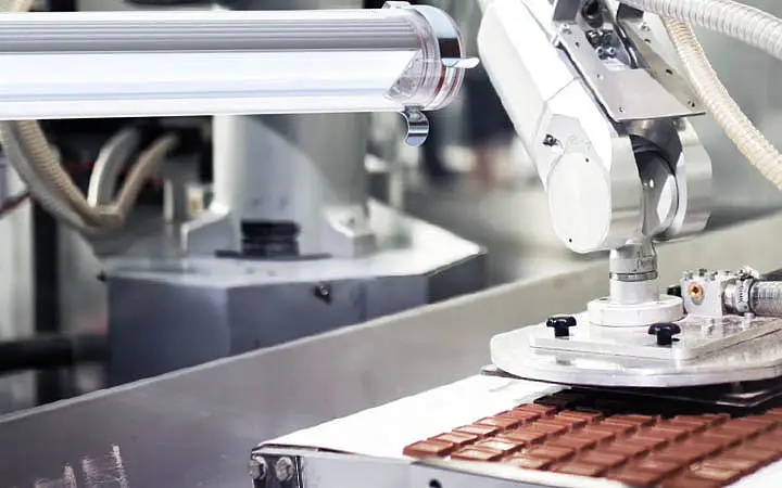
LED light manufacturing or assembly is a complicated task, but before you get started, you need master some basic knowledge and skills about the manufacturing process. There are a wide selection of equipment for LED light manufacturing. However, the production department should select the right equipment depending on the specific type of LED lights to be manufactured and the raw material to be used.
The major equipment for LED light manufacturing are as follows:
- LED PCB assembly machine
- LED lamp assembly machine
- Candlelight assembly machine for LED
- High speed LED mounting machine
- LED chip SMD mounting machine
- LED tube light assembly machine
In addition to these basic machines, some minor equipment may be required for LED light manufacturing.
- Soldering machine
- Packaging machine
- Sealing machine
- Small drilling machine
- LCR meter
- Oscilloscope
- Digital multimeter
- Lux meter
- Continuity tester
4 Steps of LED Light Manufacturing
Wafer Fabrication
The first is the fabrication of a semiconductor wafer. The material composition to be used is determined by the color of LED light, whether gallium arsenide (GaAs), gallium phosphide (GaP) or other composite materials. To mix these materials with elements such as phosphorus, gallium and arsenic, a high-temperature and high-pressure chamber is required where the materials are then purified, liquefied and pressed together to form a solution. To prevent the materials from escaping from the chamber, they are coated with a boron oxide layer to seal them off. We call this process the Czochralski crystal growth method or liquid encapsulation technique.
A rod is then dipped into a uniform solution, and as the solution cools and slowly draw the rod out of the chamber, a cylindrical crystal ingot or boule of GaAs, GaAsP or GaP is left behind on the end of the rod. After the boule is sliced into very thin semiconductor wafers, it’s time to polish the wafers. As the wafers are sanded to a smooth surface, more semiconductor layers are added to the surface. Imperfections in the crystals and polishing process will degrade the performance of LED lights.
Next, various solvents and ultrasonic are utilized to clear the wafers. Dust, dirt, flux or impurities deposited on the surface are removed in this process, which has a significant impact on the light quality of LED lights.
Adding Epitaxial Layers
The following LED light manufacturing process is the addition of epitaxial layers. As the semiconductor layers are added to the wafer surface, the wafer layers are built up over time. Some impurities or dopants need to be added in the process, which is called Liquid Phase Epitaxy method or LPE.
This technique allows the epitaxial layers with the same crystalline orientation as the underlying substrate to be biased during the deposition of the molten GaAsP. The wafer is mounted on a graphite slide that is repeatedly pushed through a molten liquid container. In order to form a sufficiently thick wafer of LPE material, various dopants are added to sequential melts or to the same melt, resulting in the layers with different electronic densities.
To alter the color or efficiency of LED lights, the wafer is then placed into a high-temperature furnace tube filled with various dopant gases such as nitrogen, zinc and ammonium. The green and yellow light emitted by LED lamps is attributed to the effect of nitrogen.
Adding Metal Contacts
Metal contacts should be defined on the wafer at the design stage. The contact pattern is determined by the combination of diodes. A light-sensitive compound called photoresist is used to clone or reproduce the contact patterns. As the wafer spins around, the resist is distributed evenly over the surface in droplets and is quickly harden by heating at 100 degrees Celsius.
The photoresist mask is then placed on the wafer to duplicate the mask pattern, while exposing the resist under ultraviolet light. Wash away the exposed areas with developer and remain the unexposed areas.
In a vaccum-sealed and high-temperature chamber, the contact metal is then evaporated onto the pattern, filling the exposed wafer areas. The metal should be heat to the point where it can vaporize, condense and adhere to the exposed wafer. To only retain the metal contacts, the photoresist need to be removed off with acetone.
Then is followed by an amalgamating process, in which nitrogen and hydrogen in the furnace chamber tightly bond together. In order to obtain a 2-inch diameter wafer, this process could have to be repeated approximately 6000 times. An individual segment separated from the wafer of diodes with a cleaving saw or a diamond saw is called a die.
Mounting and Packaging
The last step is to mount the individual dies appropriately on the package. The die is mounted on two 2-inch metal leads. In order to make an electrical contact with the lead on which it rests, the back of the wafer is covered by metal. A very thin gold wire is soldered to the second lead and stick to the patterned contacts on the surface of die by wire-bonding. In this process, a tiny needle is used to press the edge of the wire against the contact metal. Gold is so soft that it can bend easily and adhere to similar metal surfaces.
Finally, plastic is used as the sealing material for the entire assembly and the wires and die are hung in a mold filled with liquid plastic or epoxy. The shape of the mold meets the optical properties of packaging. Once the epoxy is cured, the packaging is complete.
Quality Control in LED Light Manufacturing

In general, products will be tested for quality control before packaging and shipping. With a strict quality control system, MOKOLight’s every LED product is tested multiple times to ensure that they are top-notch. In terms of quality control, there are two major concerns: the final products and the manufacturing facilities.
First of all, the test on each LED finished lamp includes the following:
- Wire bond for performance check
- Detection of current levels to obtain specific brightness
- Accurate light color test for each batch of wafers
- Heat and power breakdown test
- Mechanical damage test
- Stress testing
- Lifetime test
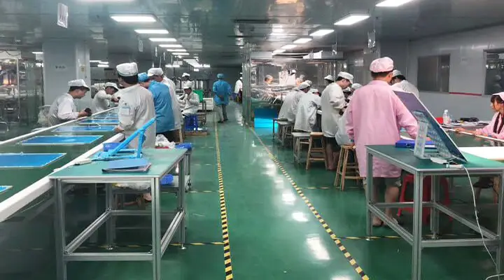
Other than the finished products, the test on the manufacturing facilities should also be involved to ensure the stability and safety of the production line. Many of the above production steps done by MOKOLight is automated, but a few are manual. They often organize the training of production safety to raise the safety awareness of their working staff.
In addition, we pay close attention to the cleanliness and maintenance of the manufacturing facilities. Some special facilities such as clean rooms are built to keep dust out. All of these checks are aimed at producing a large number of successful LED products.
Pollution Control in LED Light Manufacturing
Given the increasingly stringent requirements for LED light manufacturing, the following measures may help you manage the pollution problems in LED light manufacturing.
Some gases and fumes released during soldering are bad for humans and the environment. In order to reduce harmful gas emissions and air pollution, modern technologies and methods have been developed to replace the previous polluting technologies.
15-35% flux solids are produced in the conventional methods. With the application of new flux materials, the amount of flux solids is reduced to less than 10%, which is a major advance in pollution control.
In order to remove flux residues and packaging foams as well as reduce the emission of CFCs and methyl chloroform, various organic solvents are used to clean the circuit boards. Effective cleaners such as alcohols or ketones are applied to replace methylene chloride, trichloroethylene and perchloroethylene that have been used for many years in the electronics industry.
About LED Light Manufacturing at MOKOLight
If you are seeking for a reliable and professional LED light manufacturer, MOKOLight is the perfect choice. We have a wide array of LED lights for various applications and provide you with better quality source of light at an affordable price. Welcome to browse our website or blogs and start your LED journey right now!
